ASG SCIENTIFIC

Products

Battery/Supercapacitor Equipments

Coin Cell Battery Equipments

Pouch Cell Battery Equipments

Cylinder Cell Battery Equipments

Battery Test Equipments

Battery Pack Assembly Line

Glove Box

Ball Mill

Battery Materials

Spectroscopy Instruments

  • Higher performance all-in-one system for Raman and TCSPC/FLIM analysis
  • Confocal/3D fluorescence lifetime imaging and analysis
  • Photocurrent imaging and analysis
  • Nano Cycler
  • White Light interferometric Profiler

PicoVision-100 / PV-100 Series: Table-Top W-SEM

The PV-100 is our entry-level Tabletop SEM with a tungsten filament electron source, designed for laboratories where space is at a premium. But the small size doesn’t mean you need to compromise on features. The PV-100 comes with a 5-axis stage, and the new GUI simplifies operation while allowing both novice and expert users to easily obtain high-quality images. With an effective magnification of 70,000×, the PV-100 is ideal for routine imaging at medium and low magnifications.

Specifications

<Specifications>

Dimension(mm)

420 x 630 x 680 (W x L x H)

Electron source

Tungsten filament

Resolution

5.0 nm

Magnification

20 x ~ 300,000 x

Effective magnification

~ 70,000 x

Electron gun vacuum

10 ⁻⁶ torr

Accelerating voltage

1 ~ 30 kV

Motorized Stage

Chamber type (X,Y,Z,R,T) 50,50,30mm, 360°,
-10°~90°

Vacuum system

Rotary pump, TMP

Main System Weight (kgs)

98 kgs

PicoEye-100 / PE-100 Series: Floor Type W-SEM

The PE-100 is a compact SEM with full-size performance. Supplied with a tungsten filament source, the PE-100 has an effective magnification of over 100,000 ×. Ideal for imaging larger samples due to its oversize chamber, the PE-100 comes with an impressive set of features typically seen on more expensive microscopes, including both a Navigation Camera and a Chamber Camera for increased versatility.

Specifications

Dimension(mm)

680 x 780 x 1460 (W x L x H)

Electron source

Tungsten filament

Resolution

3.0 nm

Magnification

20 x ~ 300,000 x

Effective magnification

~ 100,000 x

Electron gun vacuum

10 ⁻⁶ torr

Accelerating voltage

1 ~ 30 kV

Motorized Stage

Chamber type (X,Y,Z,R,T)50,50,45mm, 360°, -20°~45°

Vacuum system

Rotary pump, TMP

PicoEye-300 / PE-300 Series: Entry level FE-SEM

The PE-300 is a Field Emission (Schottky) SEM with high resolution and contrast, allowing users to obtain detailed image information. The PE-30C features our innovative compact FE electron gun made of mild steel with double O-ring sealing providing fast and accurate gun axis adjustment. With superior quality and a competitive price, the PE-300 is the ideal tool when your application requires high resolution and exceptional imaging.

Specifications

Dimension(mm)

750 x 780 x 1700 (W x L x H)

Electron source

FE(Schottky)

Resolution

2.0 nm

Magnification

20 x ~ 300,000 x

Effective magnification

~ 200,000 x

Electron gun vacuum

10⁻ ¹ ⁰ torr

Accelerating voltage

0.5 ~ 30 kV

Motorized Stage

Chamber type (X,Y,Z,R,T)
50,50,45mm, 360°, -20°~45°

Vacuum system

Rotary pump, TMP, Ion pump

SEM

i.SEM: Bench top SEM

  • EM-30
  • EM-30N
  • EM-30C

ii.SEM: Full Size SEM

  • CX-200Plus

iii.Scanning ELectron Microscope for Particle Analysis

iv.Cross Section Polisher: CP-8000

v.Ion Sputter Coater: SPT-20

vi.EDS,DetectorOxford, AZtecOne with Xplore, Compact Bruker: QUANTAX Compact

vii.STEM

viii.Cool Stage: CSU-2

ix.BSE Detector:

Silicon Wafers/Substrates

We carries full range of FZ and CZ silicon wafers, the specifications and parameters comply with SEMI standards.

  • Prime, test, mechanic grades
  • Diameter from 2″ to 12″
  • Ultra thin or ultra thick
  • Crystalline orientation <100>, <111>, <110>
  • Most resistivity range
  • P type/ Boron, N type/Phos, As doped
  • Heavily doped or intrinsic wafers
  • Single side polished or double sides polished
  • Semi-standard flats or notch point
  • We keep a stock of silicon wafers with various specifications all the time. Contact us for immediate quotation and delivery.

SOI Wafers

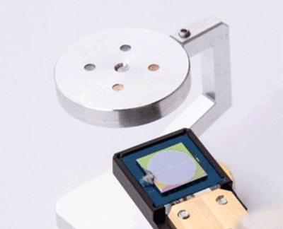
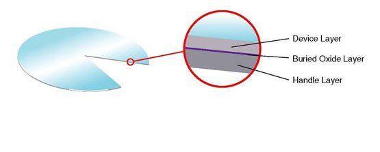
Silicon on insulator (SOI) wafers are a three layer material stack composed of the following: an active layer of prime quality silicon (DEVICE LAYER) over a buried layer (BOX) of electrically insulating material (like silicon dioxide, sapphire, silicon nitride, etc), over a bulk silicon support wafer (HANDLE LAYER).

SOI wafers provide a manufacturing solution which helps reduce power and heat while increasing the speed performance of a device. They are widely used for the fabrication of micro electro mechanical system, micro optical devices, sensors, RF switches, power devices, and advanced CMOS IC chips. SOI wafers are unique products which are often custom-built for specific end-user applications.

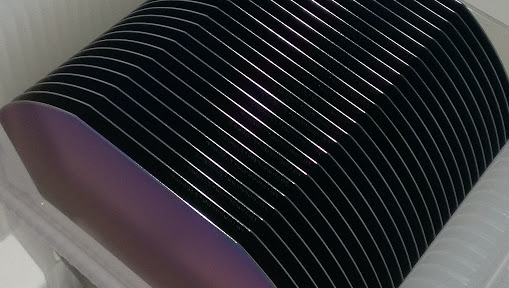
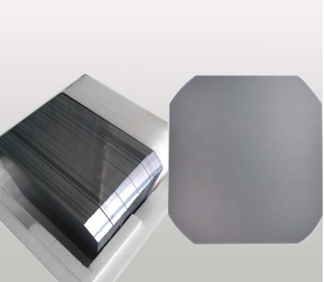
BondaTek is able to meet customer’s needs for SOI wafers with diameter from 76.2mm to 300mm. We accommodate SOI requests for development of small quantities as well as ongoing requirements.

Solar Wafer

  • Material: Monocrystalline Silicon
  • size: 125mm x 125mm and 156mm x 156mm
  • Application: Solar System
  • Packing: Carton
  • Color: Grey
  • Advantage: high quality/ short lead time/ low price/ customization
    specifications:Conductive Type: N type/ Phos doped
  • Orientation: <100>=/-3 degree
  • Resistivity: 1 – 3, 3- 6 ohm.cm
  • Bulk lifetime: >=1000us
  • Oxygen Content: <=0.1*10^18cm^3 Carbon Content: <=0.1* 10^17cm^3
  • Thickness: 200+/-20um TTV: <=25UM Saw Mark:<=15um Warp :<=40um
  • Chips: Depth <0.3mm, length <0.5mm Less than 2 chips per wafers
  • Appearance: No stain, No Pinhole and cracks by Visual Inspection Dislocation Density: =1000pcs.cm^2

Sputtering Targets

  • Metal sputtering targets
  • Alloy sputtering targets
  • Ceramic sputtering targets

Evaporation Materials

Evaporation Materials: Evaporation Materials ,also called E-beam materials ,are used for thin film deposition for a wide application. We can provide full production line.

  • Metal evaporation material
  • Oxide evaporation materials 
  • Fluoride evaporation materials 
  • Others

Electron Microscopy Products

  • Different Grids, TEM Support Films
  • TEM Window
  • Films for TEM
  • SEM Accessories
  • Atomic Force, Scanning Tunneling Microscopy
  • Transmission Electron Microscopy
  • Histology & Light Microscopy
  • Tweezers, Tools, Gadgets
  • Different Tapes, Pastes & Dispensers
  • Diamond Knife

So on…

Nanometer Materials

  • Metal powder: Nickel, Aluminum,Silver, Gold etc
  • Oxide Nano powder: Titanium, Silicon, Cobalt etc
  • Compound Nano powder: Yittria Stabalized Zirconia, Zinc Iron Oxide, Aluminum Nitride, Boron Nitride etc
  • Micro powder : Bismuth Oxide, Barium Titanate, Aluminium Oxide etc
  • OTHERS: Glass Wafers, single crystal wafers, Sapphire Wafers, SOS Wafers, GE, SRTIO3, MGO etc.,

Different Lab Furnaces & Vacuum Pumps

  • Tube Furnace
  • RTP Furnace
  • Muffle Furnace
  • Accessories

Battery Materials

  • CR20XX Coin cell cases with spring & spacer PP Separators & Celgard Separators
  • LiNiMnCoO2 Powder
  • LiFePO4 Powder
  • NMP Solvent
  • PVDF Binder
  • Coin Cell Wave Spring
  • Artificial Graphite MCMB
  • Copper Foil
  • Aluminum Foil
  • Coin Cell Spacer
  • Graphite Powder
  • 18650 Battery Cases
  • Pure Nickel Strip


  • Battery Tabs: Aluminum/Nickel
  • LMO Powder
  • Pouch Cell Case: Aluminum Laminated Film
  • LiCoO2 Powder
  • Copper Metal Foam
  • Nickel Metal Foam
  • Conical Spring /Cone Spring
  • Styrene-Butadiene Rubber Powder
  • Super P Li / Sup-p Powder
  • CMC Powder
  • Nickel Cobalt Aluminum Oxide NCA Powder
  • Polyimide Kaptons Adhesive Tape
  • PTFE Binder
  • Lithium Titanate Oxide Powder

And many others…

Different Lab Instruments

  • Lab Centrifuge
  • Magnetic Stirrer
  • Hot Plate
  • Autoclave
  • Lab Glassware
  • INCUBATOR
  • Lab Oven
  • Orbital Shaker
  • Water Bath/Ultrasonicator
  • Polarimeter
  • Vacuum Pumps
  • Microscopes
Open chat